Tools
However, we are not limited to only working within the Altium and Cadence design flows. Where required, we can take existing design-data from ANY system and carry out PCB design or signal integrity analysis. We have extensive experience in the porting of designs from one system to another, making our design services compatible with any system on the market.
Schematic Design
We can undertake schematic design entry using “Cadence Design Entry HDL” (formerly known as “Concept”), “Cadence Capture CIS” (OrCAD) or “Altium Designer”.
In addition to schematic capture, we can provide schematic libraries of components for OrCAD Capture CIS. These libraries come complete with parametric data, giving component heights, manufacturer’s part numbers, etc. For further information on our library services, please see the Library Management page.
Signal Integrity Tools
Advanced Layout Solutions is the only independent PCB design bureau that runs all its own signal integrity analyses. We own and maintain class-leading SI tools from Cadence, Keysight Technologies and Synopsys. Tool choice is heavily dependent upon the particular task at hand. For instance, the tools and approaches used for a high-speed synchronous DDR4 memory interface will be very different to those used for a SERDES link in the gigabit-per-second regime. For more information on our signal integrity services, click on the image below to be taken to our SI website.
Design For Manufacture
There are many reasons why a design, even when fully checked on a CAD system, can fail when the data is presented for manufacture. To overcome such issues and to provide a smooth transition of your boards through manufacture we have invested in multiple “Valor Enterprise 3000” systems that enable us to pinpoint any manufacturing issues on your design before the data leaves our company.
Valor ODB++ format is becoming the de facto standard for passing data between design houses and manufacturers. Unlike Gerber, this Valor format provides all the data required to manufacture your board in a single file archive.
Additionally, unlike many CAD systems that simply output a Valor ODB++ file, we provide you with verified ODB++ files. By verifying the data within the ODB++ file we ensure that the physical board data that is being used for manufacture matches the connectivity of the design exactly.
Technologies
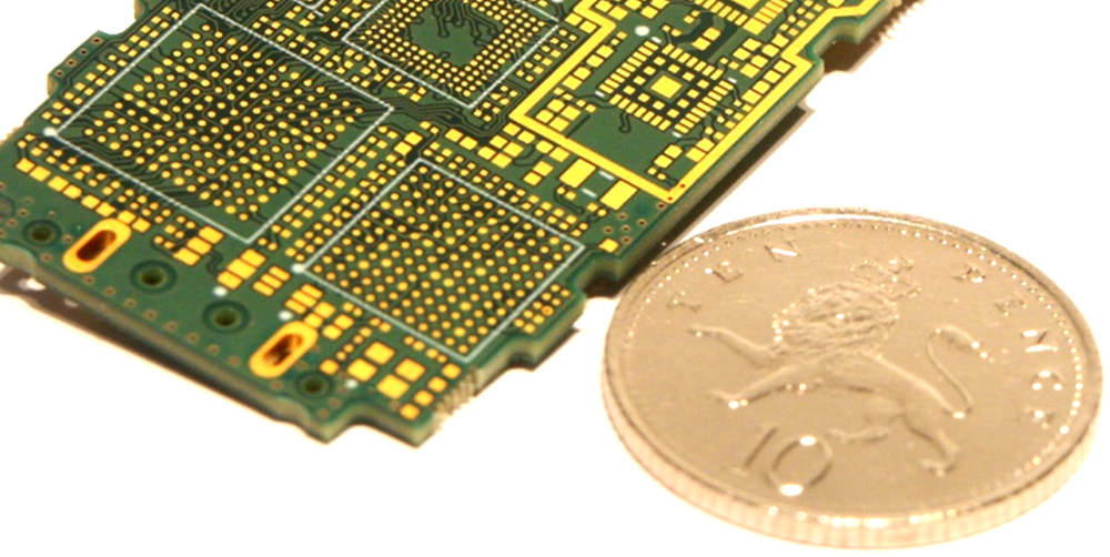
The designs that we have produced over the past decade have used every conceivable PCB technology available. Our experience working with the latest via technologies, specialist materials, high layer-counts and tight impedance control makes us confident that we can handle any design offered to us.

The correct implementation of microvias, stacked microvias and / or blind vias can resolve interconnection issues and open more design options. Our design experience combined with that of our manufacturing partners will enable you to adopt these new technologies and design methodologies with confidence.
Flex / Flex-Rigid
- Miniaturisation
- Wire harness replacement
- Reduced assembly time
- Space and weight requirements

